
When designing a printed circuit board, there are certain rules. You should place decoupling capacitors near the power pins to each chip. Your ground planes should be one gigantic fill of copper; two ground planes connected by a single trace is better known as an antenna. Analog sections should be kept separate from digital sections, and if you’re dealing with high voltage, that section needs to be isolated.
One that I hear a lot is that you must never put a 90-degree angle on a trace. Some fear the mere sight of a 90-degree angle on a PCB tells everyone you don’t know what you’re doing. But is there is really no greater sin than a 90-degree trace on a circuit board?
This conventional wisdom of eschewing 90-degree traces is baked into everything we know about circuit board design. It is the first thing you’re taught, and it’s the first thing you’ll criticize when you find a board with 90-degree traces. Do square traces actually matter? The short answer is no, but there’s still a reason we don’t do it.
RF and Capacitance Implications
When you ask someone why 90-degree traces on a printed circuit board is bad, the first reason given is RF interference.
The most-cited reason as to why you shouldn’t use square corners on traces is that electrons bunch up on the corners. This is impossible with our current understanding of physics and would break the universe. Fortunately for everyone, you can just rent test equipment that will test a circuit at 20 Gigahertz. If you’re really good, you can find that test equipment in the trash. Earlier this year, [Bil Herd] put square corners to the test by measuring the impedance of a trace that looked like a square wave. At 20 Gigahertz, the effect of square corners was minimal. At lower frequencies, the effect would be less. Don’t worry about square corners on your traces.
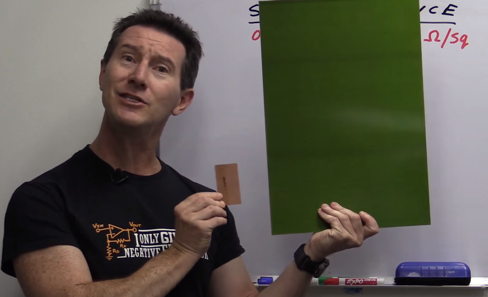
There are few, if any, implications for using 90-degree traces in respect to RF interference, but due to the nature of square corners on traces, we do bump up against the resistance of a trace. This resistance is a function of the shape of a trace, and this is known as sheet resistance. [Dave Jones] did a wonderful video on sheet resistance, and the big takeaway is that resistance of a trace is measured in Ohms per square. That’s Ohms per square, without any other dimension; a square of copper two millimeters on a side has the same resistance as a square of copper ten millimeters on a side. It’s counter-intuitive.
With that said, a 90-degree corner makes little difference in the resistance of a trace provided it is replaced with a 45-degree corner. That’s simply how triangles work. It does make a difference in the capacitance of a trace, although that effect is very minor. This has been covered by [Bil Herd] in his test of high-speed PCB design techniques and it’s been written up in EDN as a rule of thumb for high speed design. The takeaway is that square corners do effect capacitance, but it is not really an issue unless the rise time of the circuit is extremely low. The official rule of thumb is that a square corner will affect the circuit when the line width in mils is greater than five times the rise time in picoseconds. Unless you’re dealing with relatively high-speed signals — the black magic of RF or SPI busses on the order of 100 MHz, it doesn’t matter.
Acid Traps During Board Etching
Acid trap isn’t just the latest frontier of my Soundcloud, it’s also something you must take into account when manufacturing a circuit board.
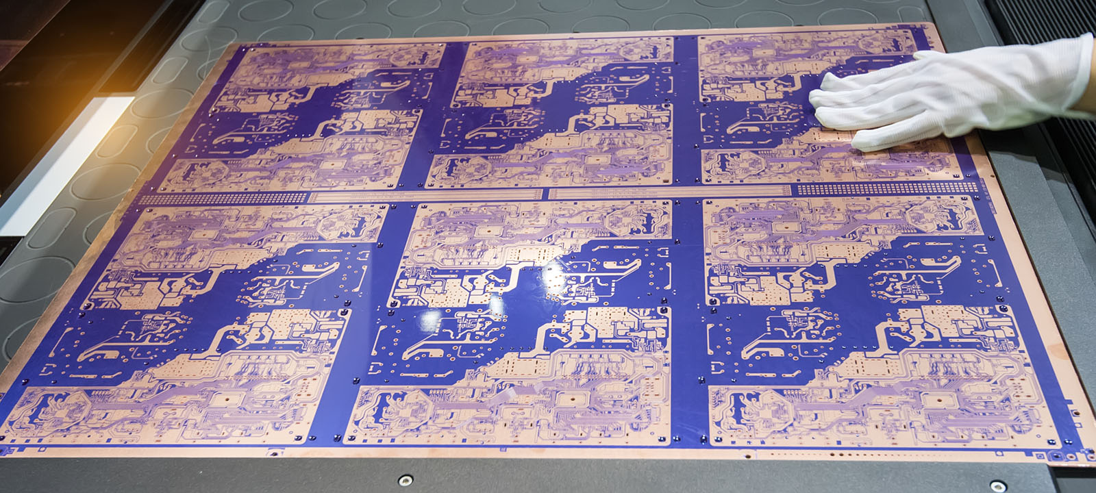
Most circuit boards begin their life as a sheet of fiberglass or other substrate covered with a layer of copper. This is the raw material for every board house, and although there are differences in the substrate, the amount of copper applied to a board, and whatever intermediary processes go into manufacturing a PCB, everything begins with copper bonded to some sort of non-conductive material. To turn this raw material into a board, a portion of the copper is masked off and the copper is removed. This can be done with laser printer toner or Ultraviolet-cured photomask, and the copper is then etched with a chemical, either Ferric chloride, Sodium persulfate, or Cupric chloride. There are many different ways to make a PCB, but they’re all strikingly similar.
When etching a board, it is possible a ‘puddle’ of the acid solution could collect at the corner of a trace. If this happens, it is possible the acid could eat away at copper underneath the photoresist. This, in turn, decreases the effective width of a trace, potentially breaking the trace entirely.
For all the tips and tricks presented to first-time board designers, the ‘acid trap’ explanation is the implicit reason for why you should not use 90-degree traces. The Eagle blog gives a top-ten routing tips for new PCB designers, and acid traps are the reason why you shouldn’t use 90-degree angles. ‘Ease of manufacturing’ is the reason for not using 90-degree traces on many articles for the tips and tricks of PCB design.
However, this tip for avoiding acid traps is decades old and the technology behind PCB manufacturing has improved greatly over the years. If your PCB fab is having problems with acid etching copper in a corner, you should probably find another board house.
So Why Does It Matter?
The know-how that goes into designing a PCB is a lot like driving a car. Anyone with a drivers license can get in a car, drive a few miles, and pick up some groceries. You can put some drinks in a cooler and go on a two hundred mile road trip no problem. The basics of driving a car are more than sufficient for 99% of your time on the road.
In driving and PCB design, there are exceptions to the majority. Popping down to Dollar General in a Chrysler Sebring is a lot different than taking your favorite supercar around the Nürburgring. Likewise, building a multi-Gigahertz circuit is much harder than connecting a Bluetooth module and an OLED display together to make a smartwatch.
The reason we don’t see square traces in most PCB designs is simply due to aesthetic convention. If it looks wrong, it is wrong. There is no specific reason why every circuit board design should shy away from 90-degree angles on traces, it’s just something that you shouldn’t do because it looks wrong.